


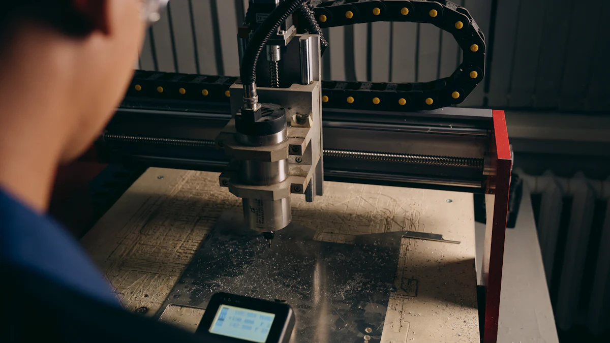
Electron beam inspection plays a crucial role in maintaining product integrity by detecting microscopic defects. This technology excels in precision and accuracy, making it indispensable in advanced semiconductor manufacturing processes. By utilizing high-energy electron beams, it scans wafer surfaces and examines various layers of integrated circuits. This method provides high-resolution imaging, allowing for precise defect detection and characterization. The ability to detect nanometer-scale defects ensures superior quality in production. As a result, electron beam inspection has become a vital component in quality control, enhancing the overall quality of products across industries.
Key Takeaways
- Electron beam inspection provides exceptional precision and accuracy, crucial for maintaining product specifications in industries like semiconductor manufacturing.
- This technology enhances reliability in quality assessments by delivering high-resolution imaging, allowing manufacturers to make informed decisions about product quality.
- Non-destructive testing capabilities of electron beam inspection preserve the integrity of materials, making it ideal for sensitive sectors such as aerospace and electronics.
- By reducing waste and rework, electron beam inspection proves to be a cost-effective solution, leading to significant long-term savings in production costs.
- E-beam inspection excels in identifying subsurface flaws, ensuring safety and reliability in critical components, particularly in the aerospace industry.
- Early detection of defects through electron beam inspection helps prevent costly recalls and repairs, enhancing product lifecycle and customer satisfaction.
- Adopting electron beam inspection can improve product reliability and efficiency, providing manufacturers with a competitive advantage in the market.
High Precision and Accuracy
Precision in Measurement
E-beam inspection stands out for its exceptional precision in measurement. This technology utilizes high-energy electron beams to detect minute variations that traditional optical methods might miss. The ability to identify these subtle differences is crucial in maintaining product specifications, especially in industries where even the smallest deviation can lead to significant issues. For instance, in semiconductor manufacturing, e-beam inspection ensures that each component adheres to the exact design parameters, thereby upholding the quality of the final product.
Accuracy in Results
The accuracy of e-beam inspection results significantly reduces errors in quality assessments. By providing high-resolution imaging, this advanced inspection technology enhances the reliability of inspection data. Manufacturers can trust the data to make informed decisions about product quality and defect detection. This accuracy is particularly important in the critical dimension measurement of semiconductor devices, where precise measurements are essential for device performance. E-beam inspection’s superior resolution and sensitivity ensure that even the smallest defects are detected, preventing potential failures and ensuring the highest quality standards are met.
Non-Destructive Testing Capabilities
Electron beam welding offers significant advantages in non-destructive testing capabilities, making it a preferred choice in various industries. This method allows for the inspection of materials without causing any damage, ensuring that the structural integrity of the sample remains intact. The ability to conduct thorough inspections without altering the material is crucial, especially in sensitive sectors.
Preservation of Sample Integrity
Non-destructive methods, such as electron beam welding, play a vital role in industries where maintaining sample integrity is paramount. In aerospace and electronics, for instance, the need to preserve the original state of components during inspection is critical. These industries rely on electron beam welding to ensure that their products meet stringent safety and performance standards without compromising the material’s integrity.
Scientific Research Findings: Scanning Electron Microscope (SEM) is widely used for non-destructive detection of micrometric internal features within electronic systems. This application highlights the importance of non-destructive methods in preserving sample integrity.
Cost-Effectiveness

Electron beam welding not only preserves sample integrity but also proves to be cost-effective. By reducing waste and rework, this method minimizes unnecessary expenses. Manufacturers can avoid the costs associated with replacing or repairing damaged components, leading to significant savings over time. The long-term savings in production costs make electron beam welding an economically viable option for quality control.
Scientific Research Findings: The use of electron beam inspection systems in chip manufacturing expedites time-to-market by identifying critical defects early in the process. This real-time analysis capability reduces the need for costly rework and enhances overall efficiency.
Enhanced Detection of Defects
Identifying Subsurface Flaws
E-beam inspection excels in identifying subsurface flaws, which are often hidden from traditional inspection methods. This capability proves crucial in industries where safety and reliability are paramount. For example, in the aerospace sector, detecting defects beneath the surface of critical safety components can prevent catastrophic failures. E-beam inspection systems can identify a wide range of defect types, including voids, cracks, and inclusions, that might compromise the structural integrity of these components. By providing a comprehensive understanding of these defects, e-beam inspection ensures that products meet stringent safety standards.
Scientific Insight: E-beam inspection has become one of the most important tools for rapid yield ramp in the semiconductor industry due to its ability to detect a wide range of defects in-line soon after their formation.
Early Detection and Prevention
The early detection and prevention of defects play a vital role in maintaining product quality and reliability. E-beam inspection systems offer manufacturers the ability to identify defects at an early stage, preventing them from progressing into more significant issues. This proactive approach helps in avoiding product failures that could lead to costly recalls or repairs. By addressing defects early, manufacturers can enhance the product lifecycle and improve customer satisfaction. The impact of early defect detection extends beyond immediate cost savings; it also contributes to a brand’s reputation for delivering high-quality products.
Industry Application: The e-beam inspection system plays a vital role in expediting time-to-market for cutting-edge electronic devices by offering a comprehensive understanding of critical defects during the chip manufacturing process.
Conclusion
Electron beam inspection offers numerous benefits that significantly enhance quality control processes. It provides high-resolution imaging and precise defect detection, ensuring that even the smallest flaws are identified and addressed. This technology plays a crucial role in maintaining high yield rates and product quality, especially in semiconductor manufacturing. As industries continue to demand smaller and more efficient devices, the importance of electron beam inspection will only grow. By adopting this advanced inspection method, manufacturers can improve product reliability and efficiency, ultimately leading to greater customer satisfaction and competitive advantage.