


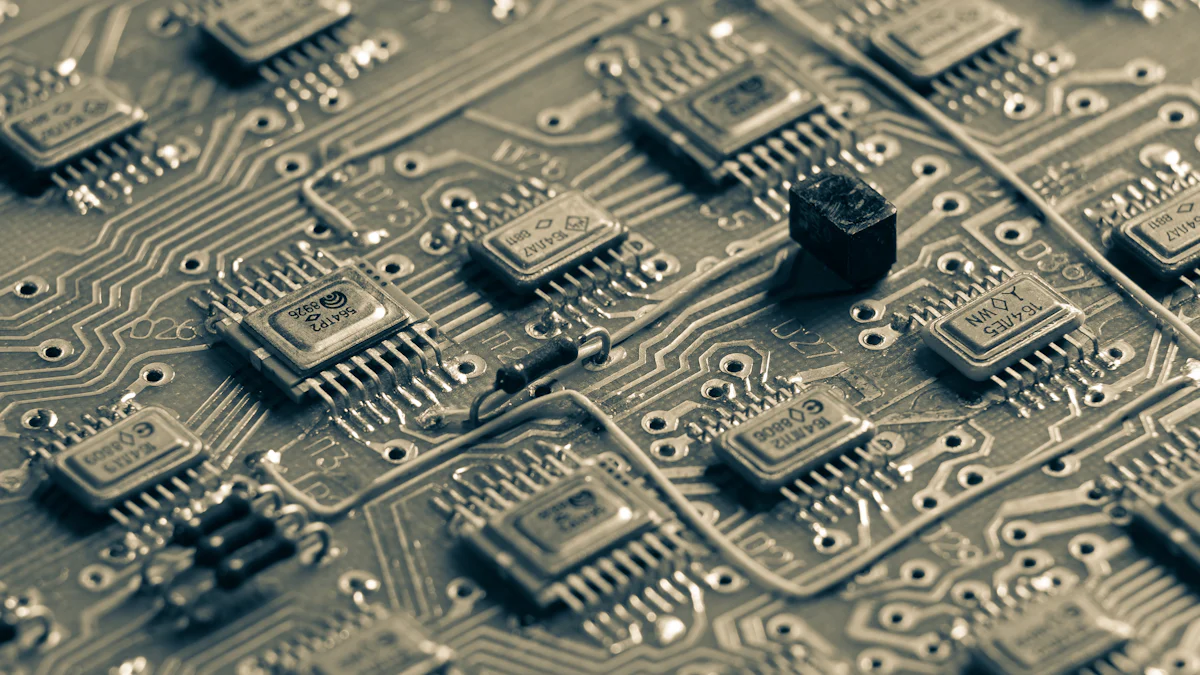
Electron beam etching redefines precision in material processing. This advanced technique achieves nanometer-scale accuracy, making it indispensable for applications requiring intricate details. Unlike traditional methods, it uses focused electron beams to selectively remove material, ensuring minimal waste and cleaner results. The etching process operates in a vacuum environment, reducing contamination and enhancing reliability. Its ability to handle diverse materials, from metals to polymers, further highlights its versatility. While some methods struggle with complex geometries, electron beam etching excels, offering unmatched control and adaptability for cutting-edge industries.
Key Takeaways
- Electron beam etching achieves nanometer-scale precision, making it ideal for applications requiring intricate details and complex geometries.
- This technique operates in a vacuum environment, which minimizes contamination and enhances the reliability of the etching process.
- Electron beam etching significantly reduces production time by allowing for selective material removal without extensive additional steps.
- The focused nature of the electron beam minimizes material waste, making it an environmentally friendly choice compared to traditional chemical etching methods.
- Electron beam etching is compatible with a wide range of materials, including metals, semiconductors, and polymers, ensuring versatility across various industries.
- This advanced etching method is crucial for cutting-edge industries like electronics, aerospace, and medical devices, where precision and reliability are paramount.
- By providing cleaner, faster, and more accurate results, electron beam etching sets a new standard for advanced material processing.
Unparalleled Precision for Microscopic Applications
Subatomic-Level Accuracy
Electron beam etching achieves nanometer-scale precision by utilizing a focused beam of electrons. These electrons interact with the material at an atomic level, enabling the removal of specific areas with exceptional accuracy. This process ensures that even the smallest features can be etched without compromising the surrounding material. The ability to control the energy and dose of the electron beam further enhances its precision, making it ideal for applications requiring intricate details.
When compared to ion beam etching, electron beam etching offers a significant advantage in resolution. Ion beam etching relies on charged particles, which can result in broader etching profiles and less defined edges. Plasma etching, on the other hand, uses plasma technology, which is effective for larger-scale applications but lacks the fine detail achievable with electron beams. Electron beam etching stands out as the preferred choice for tasks demanding subatomic-level accuracy.
Ideal for Complex Geometries
Electron beam etching excels in creating intricate patterns and complex geometries. The focused electron beam can be directed with high precision, allowing for the etching of detailed designs that would be challenging with other methods. This capability makes it indispensable for industries such as electronics and nanotechnology, where complex structures are often required.
Laser etching, while effective for certain applications, struggles to achieve the same level of detail. The larger beam size and heat generation associated with lasers can limit their ability to produce fine features. In contrast, electron beam etching operates in a vacuum environment, minimizing thermal effects and ensuring cleaner, more precise results. This advantage allows it to handle even the most demanding geometric requirements with ease.
Superior Efficiency in Material Processing
Faster Processing Times
Electron beam etching significantly reduces production time by utilizing a highly focused electron beam. This precision allows for the selective removal of material without the need for additional steps, streamlining the overall process. The ability to control the energy and dose of the electron beam ensures consistent results, minimizing the need for rework or adjustments.
When compared to wet chemical etching, electron beam etching offers a faster and more controlled process. Wet chemical etching often requires multiple stages and extensive cleaning, which can slow down production. Similarly, ion beam etching, while effective for certain applications, operates at a slower pace due to its reliance on charged particles and broader etching profiles. Electron beam etching, with its precise and efficient approach, stands out as a superior choice for industries requiring rapid and accurate material processing.
Minimal Material Waste
The focused nature of electron beam etching plays a crucial role in reducing material waste. By targeting specific areas with nanometer-scale accuracy, this technique ensures that only the necessary material is removed. This precision not only conserves resources but also enhances the quality of the final product by avoiding damage to surrounding areas.
Environmental benefits further highlight the advantages of electron beam etching. Unlike chemical etching methods, which often involve hazardous substances and generate significant waste, electron beam etching operates in a vacuum environment. This setup minimizes contamination and eliminates the need for harmful chemicals. Plasma etching, another dry etching technique, can also produce waste in the form of byproducts from plasma reactions. In contrast, electron beam etching offers a cleaner and more sustainable alternative, making it an environmentally responsible choice for advanced material processing.
Versatility Across Industries and Materials
Compatibility with Diverse Materials
Electron beam etching demonstrates remarkable adaptability when working with a wide range of materials. This technique effectively processes metals, semiconductors, and polymers by utilizing a focused electron beam to remove material with nanometer-scale precision. Metals benefit from the high energy of the electron beam, which allows for clean and precise etching without compromising structural integrity. Semiconductors, essential in electronics, achieve intricate patterns through this method, ensuring optimal performance in devices. Polymers, often challenging for other etching techniques, respond well to the controlled energy of electron beams, enabling detailed patterning without degradation.
Other methods, such as plasma etching, face limitations when dealing with certain materials. Plasma etching relies on ionized gases, which can lead to uneven results on polymers or cause unwanted reactions with sensitive materials. Similarly, reactive ion beam etch struggles with achieving uniformity across diverse surfaces, particularly when handling materials with varying densities. Chemically assisted ion beam etch, while effective for some applications, often requires additional steps to address compatibility issues. Electron beam etching overcomes these challenges, offering a versatile solution for industries requiring precision across multiple material types.

Applications in Cutting-Edge Industries
Electron beam etching plays a pivotal role in advancing industries that demand high precision and reliability. In electronics, this technique enables the creation of intricate circuits and components essential for modern devices. The ability to achieve nanoscale patterns ensures that electronic devices remain compact and efficient. Aerospace applications benefit from the precision of electron beam etching, which allows for the fabrication of lightweight yet durable components. Medical devices, requiring both accuracy and biocompatibility, also rely on this method to produce intricate designs for implants and diagnostic tools.
Traditional methods often fall short in meeting the demands of these advanced applications. Plasma etching, while effective for large-scale processes, lacks the fine detail required for cutting-edge industries. Reactive ion beam etch, though precise, can be slower and less efficient for complex geometries. Chemically assisted ion beam etch introduces additional chemical processes, which may compromise the purity of the final product. Electron beam etching surpasses these limitations, providing a cleaner, faster, and more reliable solution for industries at the forefront of innovation.
Conclusion
Electron beam etching redefines material processing by combining precision, efficiency, and versatility. Its ability to achieve nanoscale resolution ensures intricate designs with unmatched accuracy. The process minimizes waste and accelerates production, making it a superior alternative to reactive ion etching for industries requiring high-performance solutions. Additionally, its adaptability across diverse materials and applications highlights its role in advancing technology. By enabling fine control over nanostructures and delivering consistent results, electron beam etching remains a cornerstone for innovation. As industries evolve, this technique will continue to set the standard for advanced etching methods.