


Thin film deposition serves as a cornerstone in semiconductor manufacturing, enabling the creation of ultra-thin, functional layers that are critical for modern electronics. This process allows manufacturers to deposit materials with exceptional precision, ensuring the performance and reliability of devices like transistors, memory chips, and integrated circuits. The global thin film deposition systems market, valued at $13.2 billion in 2023, reflects its growing importance, with projections reaching $19.5 billion by 2028. These advancements drive innovation in industries ranging from consumer electronics to renewable energy, showcasing the indispensable role of thin film deposition in shaping technological progress.
Key Takeaways
- Thin film deposition is essential for creating ultra-thin layers in semiconductor manufacturing, enabling the production of advanced electronic devices.
- Precision in thin film deposition allows for miniaturization, which is crucial for developing smaller, faster, and more efficient components.
- Different types of layers—conductive, semiconductor, and insulating—are created through thin film deposition, each serving a vital role in device functionality.
- Techniques like Atomic Layer Deposition (ALD) provide atomic-level control, making them ideal for applications requiring extreme precision.
- Thin film deposition contributes to sustainability in manufacturing by reducing material waste and supporting energy-efficient technologies.
- The growing market for thin film deposition systems highlights its increasing importance across various industries, including consumer electronics and renewable energy.
- Investing in advanced thin film deposition technologies can drive innovation and improve the performance of modern electronic devices.
What Is Thin Film Deposition?
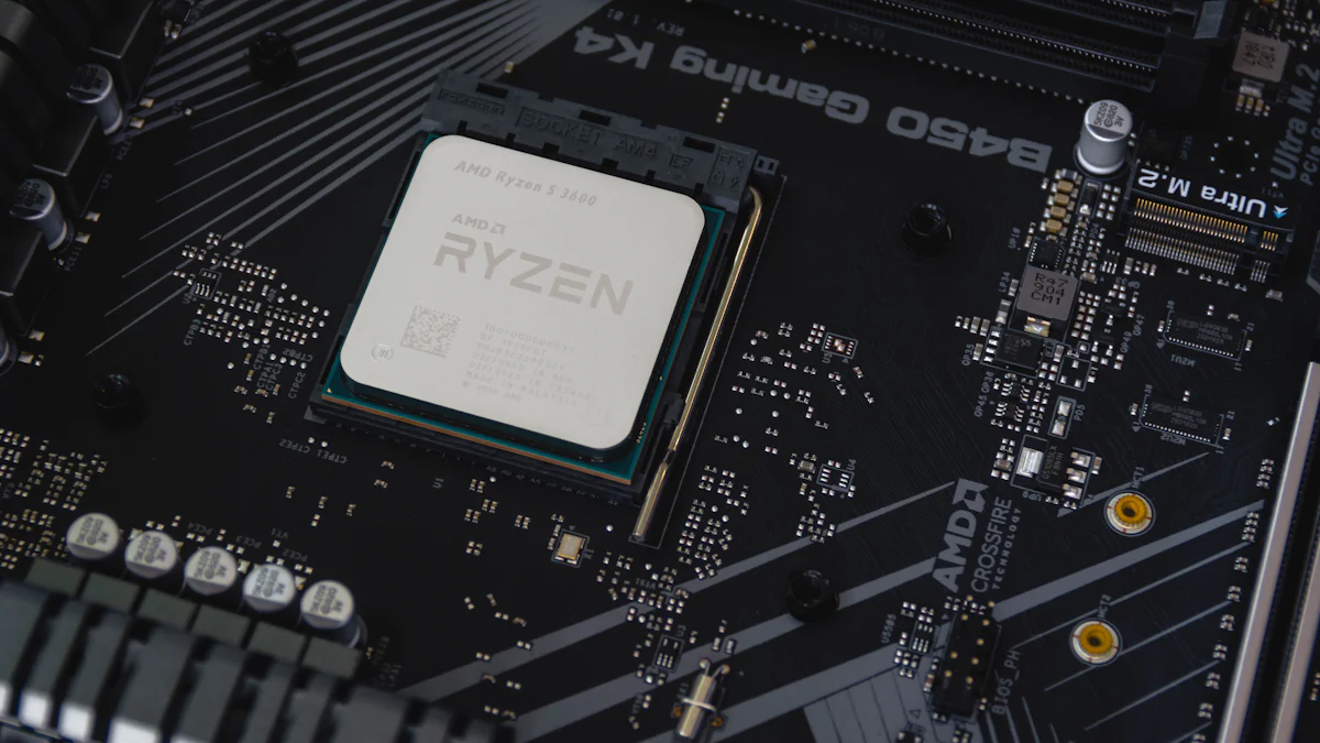
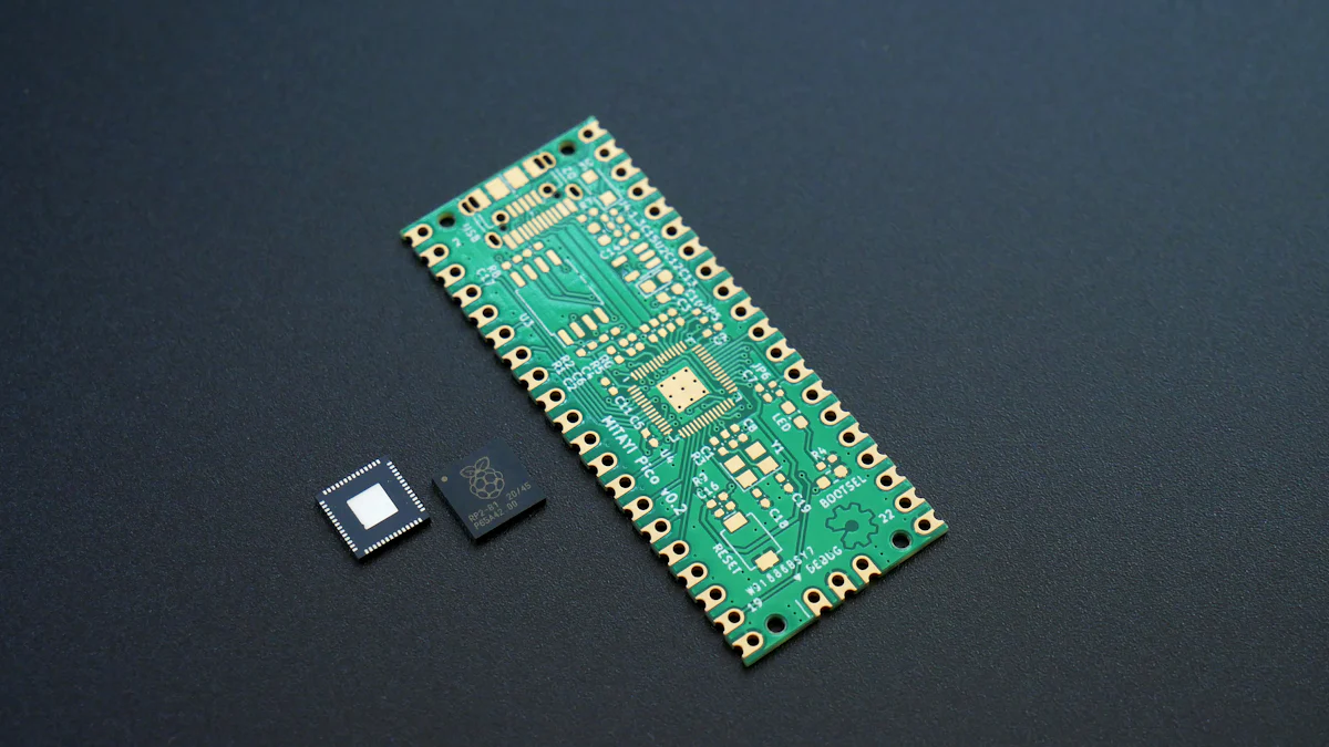
Thin film deposition refers to the process of creating extremely thin layers of material on a substrate. These layers, often measured in nanometers, serve as the foundation for many modern technologies, particularly in semiconductor manufacturing. By depositing materials with high precision, this technique enables the production of components that are essential for electronic devices, such as transistors, memory chips, and integrated circuits.
Definition and Purpose
Thin film deposition involves the controlled application of material onto a surface to achieve specific properties or functionalities. The purpose of this process extends beyond simply adding a layer. It allows manufacturers to tailor the electrical, optical, and mechanical characteristics of a device. For instance, in semiconductor manufacturing, thin films act as conductors, insulators, or semiconductors, depending on the material used and the intended application.
The origins of thin film technology date back to ancient times when metallic films were applied to artifacts for decorative purposes. Today, the process has evolved into a highly sophisticated technique. Modern methods, such as Chemical Vapor Deposition (CVD) and Physical Vapor Deposition (PVD), enable the creation of high-purity films with exceptional uniformity. These advancements have made thin film deposition indispensable in industries like electronics, renewable energy, and even aerospace.
“Thin film deposition is not just a manufacturing process; it is the backbone of technological innovation,” as highlighted by industry experts.
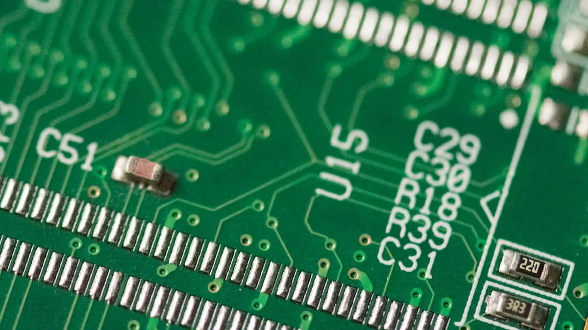
Types of Layers Created in Semiconductor Manufacturing
In semiconductor manufacturing, thin film deposition produces three primary types of layers:
- Conductive Layers: These layers allow the flow of electrical current and are crucial for creating circuits. Materials like copper and aluminum are commonly used for this purpose.
- Semiconductor Layers: These layers control the flow of electricity and form the core of devices like transistors. Silicon, a widely used material, serves as the foundation for most semiconductor layers.
- Insulating Layers: These layers prevent electrical currents from passing through unintended areas. They play a vital role in ensuring the reliability and efficiency of semiconductor devices. Silicon dioxide and silicon nitride are popular choices for insulating layers.
Each type of layer contributes to the overall functionality of semiconductor devices. For example, conductive layers enable connections between components, while insulating layers protect against short circuits. Semiconductor layers, on the other hand, regulate the behavior of electrical signals, making them essential for device operation.
The increasing demand for advanced electronics has driven significant investments in thin film deposition technologies. Techniques like Atomic Layer Deposition (ALD) have gained popularity due to their ability to produce ultra-thin films with atomic-level precision. This precision is critical for achieving the miniaturization required in modern devices, such as smartphones and wearable technology.
Why Is Thin Film Deposition Important in Semiconductor Manufacturing?
Thin film deposition plays a pivotal role in the advancement of semiconductor technology. Its ability to create ultra-thin, precise layers has revolutionized the production of semiconductors, enabling the development of smaller, faster, and more efficient devices. This section explores the key reasons why thin film deposition is indispensable in semiconductor manufacturing.
Precision and Miniaturization
The demand for compact and high-performing electronic devices has driven the need for precision in semiconductor manufacturing. Thin film deposition enables manufacturers to deposit materials with atomic-level accuracy, ensuring uniformity and consistency across layers. This precision is critical for creating intricate structures required in modern semiconductors.
Miniaturization, a cornerstone of technological progress, relies heavily on thin film deposition. By producing ultra-thin layers, this process supports the development of smaller components without compromising functionality. For instance, techniques like Atomic Layer Deposition (ALD) allow for the creation of films as thin as a single atom, meeting the stringent requirements of advanced electronics. The ability to achieve such precision has made thin film deposition a cornerstone of innovation in industries ranging from consumer electronics to aerospace.
“Miniaturization would not be possible without the precision offered by thin film deposition,” according to industry experts.
Material Properties and Functionality
Thin film deposition provides unparalleled control over material properties, enabling manufacturers to tailor films for specific applications. In semiconductor manufacturing, this control is essential for achieving desired electrical, optical, and mechanical characteristics. For example, conductive layers facilitate the flow of electricity, while insulating layers prevent unwanted current leakage. Semiconductor layers, on the other hand, regulate electrical signals, forming the backbone of thin film devices.
The versatility of thin film applications extends beyond semiconductors. Industries such as photovoltaics and optoelectronics benefit from the ability to customize material properties. Thin film deposition techniques, including Chemical Vapor Deposition (CVD) and Physical Vapor Deposition (PVD), allow for the creation of high-purity films with exceptional functionality. These advancements have expanded the scope of thin film applications, making them integral to modern technology.
Reliability and Performance
Reliability and performance are critical factors in semiconductor manufacturing. Thin film deposition ensures the durability and efficiency of semiconductor devices by creating layers with consistent quality. The uniformity of thin films minimizes defects, reducing the risk of device failure. This reliability is particularly important in applications where performance cannot be compromised, such as medical devices and aerospace systems.
The performance of semiconductors depends on the precise engineering of their layers. Thin film deposition enables the optimization of material properties, enhancing the overall functionality of devices. For instance, the use of advanced materials in thin film deposition has improved the efficiency of solar panels and the performance of microprocessors. These innovations highlight the indispensable role of thin film deposition in driving technological progress.
Common Methods of Thin Film Deposition
Thin film deposition relies on various advanced techniques to create precise and functional layers. Each method offers unique advantages, making them suitable for specific applications in semiconductor manufacturing and beyond. Below are the three most commonly used deposition techniques.
Physical Vapor Deposition (PVD)
Physical Vapor Deposition (PVD) is a widely adopted thin film deposition method. It involves the physical transfer of material from a solid or liquid source to a substrate in a vacuum environment. This technique ensures high-purity films with excellent adhesion and uniformity. PVD is particularly effective for creating conductive and protective layers in semiconductors, electronics, and even aerospace components.
The PVD process includes methods like sputtering and evaporation. In sputtering, ions bombard a target material, causing atoms to eject and deposit onto the substrate. Evaporation, on the other hand, involves heating the material until it vaporizes and condenses on the substrate. These approaches allow manufacturers to achieve precise control over film thickness and composition.
“PVD has revolutionized industries by enabling the production of durable, high-performance coatings,” according to industry analysts.
PVD’s versatility extends to applications in medical devices, automotive parts, and renewable energy technologies. Its ability to produce wear-resistant and corrosion-resistant coatings makes it indispensable in these sectors. As technology advances, PVD continues to evolve, offering improved efficiency and broader applications.
Chemical Vapor Deposition (CVD)
Chemical Vapor Deposition (CVD) is another essential thin film deposition technique. It involves the chemical reaction of gaseous precursors on a substrate’s surface, forming a solid thin film. This method is highly valued for its ability to produce uniform, high-quality films with excellent conformality, even on complex geometries.
CVD is commonly used to create semiconductor layers, insulating films, and protective coatings. Materials like silicon dioxide, silicon nitride, and tungsten are frequently deposited using this technique. The process operates at elevated temperatures, which facilitates the formation of dense and defect-free films.
One of the key advantages of CVD is its scalability. Manufacturers can use it to produce thin films on a large scale, making it ideal for industrial applications. Additionally, CVD supports the creation of films with tailored properties, such as electrical conductivity or optical transparency, enhancing the functionality of semiconductor devices.
“CVD has become a cornerstone of modern semiconductor manufacturing due to its precision and adaptability,” as noted by experts in the field.
Emerging trends in CVD include the integration of automation and eco-friendly processes. These innovations aim to reduce energy consumption and environmental impact while maintaining high performance. As industries prioritize sustainability, CVD remains a critical tool in achieving these goals.
Atomic Layer Deposition (ALD)
Atomic Layer Deposition (ALD) represents the pinnacle of precision in thin film deposition. This technique involves the sequential application of gaseous precursors in a self-limiting manner, ensuring atomic-level control over film thickness and composition. ALD is particularly suited for applications requiring ultra-thin, conformal coatings.
The demand for atomic layer deposition has surged with the growing need for miniaturization in electronics. ALD enables the production of films as thin as a single atom, meeting the stringent requirements of advanced semiconductor devices. Its ability to coat intricate structures uniformly makes it superior to other deposition techniques like CVD and PVD in certain scenarios.
ALD is widely used in the fabrication of transistors, memory devices, and sensors. It also plays a crucial role in emerging technologies, such as flexible electronics and quantum computing. The technique’s precision and versatility have made it a preferred choice for industries seeking to push the boundaries of innovation.
“ALD offers unmatched control over material properties, making it a game-changer in thin film deposition,” according to leading researchers.
As industries continue to demand smaller and more efficient components, ALD’s importance will only grow. Its potential to reduce costs while enhancing performance positions it as a key driver of technological progress.
These deposition techniques—PVD, CVD, and ALD—form the backbone of thin film deposition processes. Each method offers distinct advantages, catering to the diverse needs of semiconductor manufacturing and other industries. By leveraging these advanced techniques, manufacturers can achieve the precision, reliability, and functionality required for modern technologies.
The Role of Thin Film Deposition in Modern Electronics
Thin film deposition has become a cornerstone in the development of modern electronics. Its ability to create ultra-thin, precise layers has enabled groundbreaking advancements in technology. From powering high-performance components to supporting sustainable manufacturing practices, thin film deposition continues to shape the future of electronics.
Enabling Advanced Technologies
Thin film deposition plays a pivotal role in enabling advanced electronic components. By allowing manufacturers to deposit materials with atomic-level precision, it supports the creation of semiconductors that power devices like smartphones, laptops, and wearable technology. These components rely on thin film deposition to achieve the miniaturization and efficiency required for modern applications.
The process also facilitates the development of high-performance components used in industries such as aerospace, healthcare, and renewable energy. For example, thin film applications in solar panels enhance their efficiency by optimizing light absorption. Similarly, optical coatings produced through thin film deposition improve the performance of lenses and sensors in medical imaging devices.
Industry experts emphasize, “High-performance applications, such as semiconductors and optical coatings, require precision and customization, which fuels the need for specialized deposition services.”
Thin film deposition techniques, such as Atomic Layer Deposition (ALD), have proven indispensable in meeting the stringent demands of advanced technologies. ALD enables the production of films as thin as a single atom, ensuring uniformity and consistency across intricate structures. This level of precision is critical for achieving the reliability and functionality expected from cutting-edge devices.
Supporting Sustainability in Semiconductor Manufacturing
Sustainability has become a key focus in semiconductor manufacturing, and thin film deposition contributes significantly to this goal. By enabling the efficient use of materials, it reduces waste and minimizes the environmental impact of production processes. Techniques like Chemical Vapor Deposition (CVD) and Physical Vapor Deposition (PVD) allow manufacturers to create high-quality films with minimal resource consumption.
Thin film deposition also supports the development of energy-efficient technologies. For instance, it plays a crucial role in the production of semiconductors used in energy-saving devices, such as LED lighting and power-efficient microprocessors. These innovations help reduce energy consumption, aligning with global efforts to combat climate change.
Emerging trends in thin film applications include the use of eco-friendly materials and processes. Manufacturers are increasingly adopting deposition methods that prioritize sustainability without compromising performance. This shift reflects the growing recognition of thin film deposition as a tool for achieving both technological and environmental goals.
“Thin film deposition is not just about innovation; it is about creating a sustainable future,” as noted by industry leaders.
By combining precision, efficiency, and environmental responsibility, thin film deposition continues to drive progress in semiconductor manufacturing. Its role in supporting sustainability highlights its importance not only as a technological enabler but also as a contributor to global environmental initiatives.
Conclusion
Thin film deposition serves as a cornerstone in advancing semiconductor technology. By enabling the creation of precise and functional layers, it drives the performance and reliability of modern electronic devices. Its applications extend beyond semiconductors, contributing to innovations in optics, medical devices, and energy solutions. The continuous evolution of thin film applications ensures its relevance in addressing challenges like miniaturization and sustainability. As industries demand higher precision and efficiency, thin film deposition remains indispensable in shaping the future of technology and manufacturing.