


Focused electron beam technology serves as a cornerstone in the realm of 3D nanoprinting. This advanced technique harnesses the power of electrons to manipulate materials at the nanoscale with unparalleled precision. By directing a concentrated beam of electrons, scientists can fabricate intricate 3D structures layer by layer. This method has revolutionized nanoprinting, enabling the creation of complex geometries and enhancing material properties. The transformative potential of focused electron beam lies in their ability to produce high-resolution patterns, paving the way for innovations across various industries.
Key Takeaways
- Focused electron beam technology enables the creation of intricate 3D structures with unmatched precision, revolutionizing the field of nanoprinting.
- The ability to manipulate materials at the nanoscale allows for the fabrication of complex geometries that enhance material properties across various industries.
- Operators must ensure proper equipment setup and material preparation to achieve high-quality results in 3D nanoprinting.
- Safety and precision are critical; regular calibration and adherence to safety protocols are essential for successful operation.
- Despite its advantages, challenges such as high equipment costs and material limitations must be addressed to broaden the adoption of focused electron beam technology.
- Continuous advancements in electron beam technology promise to unlock new applications and improve scalability in nanoprinting.
- By following best practices and troubleshooting common issues, operators can maximize the potential of focused electron beam technology in their projects.
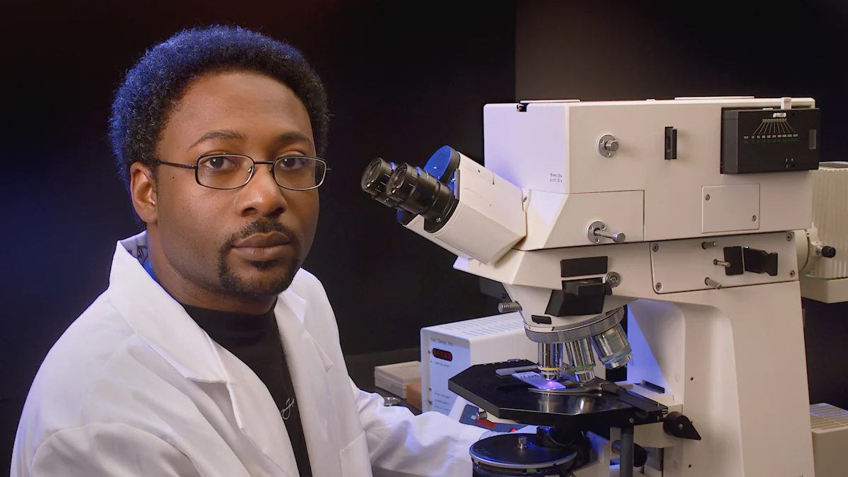
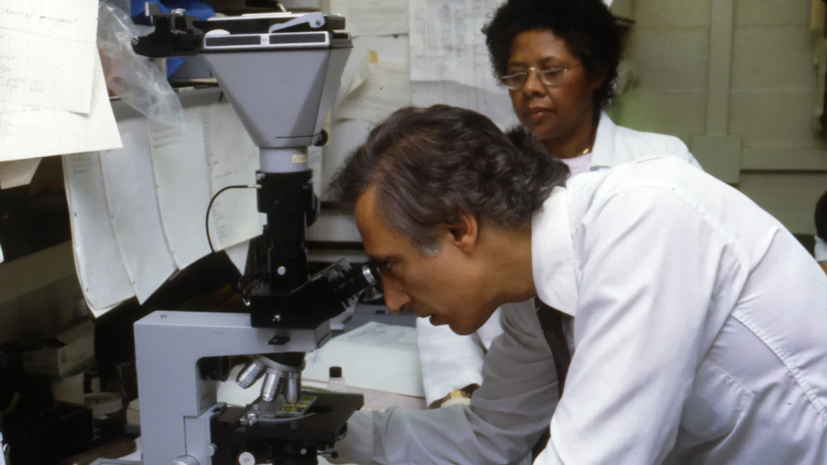
Understanding Focused Electron Beam Technology
Basic Principles of Electron Beam Technology
How Does Electron Beam Generated?
Focused electron beam technology begins with the generation of electrons. Scientists use an electron gun to emit electrons, which are then accelerated through a vacuum. This process creates a highly focused electron beam. The beam’s precision allows it to target specific areas on a material’s surface. By controlling the beam’s focus and intensity, researchers can manipulate materials at the nanoscale. This capability forms the foundation of 3D nanoprinting.
Interaction with Materials at the Nanoscale
Once generated, the focused electron beam interacts with materials at the nanoscale. The beam’s energy causes atoms in the material to rearrange, enabling precise modifications. This interaction is crucial for 3D nanoprinting, as it allows for the creation of intricate structures. The beam’s ability to induce changes at such a small scale makes it invaluable for applications requiring high precision. For instance, scientific research findings highlight the use of focused electron beam in shaping nanodevices and fabricating nanoholes in materials like multiwalled carbon nanotubes.
Role in 3D Nanoprinting
Precision and Control in Material Manipulation
In 3D nanoprinting, precision and control are paramount. Focused electron beam offers unparalleled accuracy in material manipulation. By directing the beam with exactitude, scientists can achieve complex geometries that were previously unattainable. This precision is essential for 3D-FEBID, where layer-by-layer deposition builds up the desired structure. The ability to control the beam’s path and intensity ensures that each layer aligns perfectly, resulting in high-resolution 3D structures.
Applications in Various Industries
The versatility of focused electron beam technology extends its applications across multiple industries. In optoelectronics, for example, 3D nanoprinting enables the fabrication of components with enhanced optical properties. The medical field benefits from the technology’s precision in creating nanoscale devices for diagnostics and treatment. Additionally, scientific research findings indicate that focused electron beam induced deposition (FEBID) plays a significant role in advanced scanning probe microscopy (SPM) applications. This technique allows for controlled 3D nanoscale deposition, expanding the capabilities of traditional manufacturing methods.
Applications of 3D-FEBID also include the production of 3D nanomagnets and other functional nanostructures. These innovations demonstrate the transformative potential of focused electron beam in nanoprinting. As industries continue to explore the possibilities of 3D nanoprinting technology, the demand for precise and adaptable techniques like FEBID will likely increase.
Advantages of Using Focused Electron Beam in Nanoprinting
High Precision and Resolution
Focused electron beam technology stands out in the realm of 3D nanoprinting due to its exceptional precision and resolution. This technology allows for the creation of intricate 3D nanostructures with remarkable accuracy. By manipulating materials at the atomic level, focused electron beam enables the fabrication of complex geometries that were once thought impossible.
Achieving Complex Geometries
The ability to achieve complex geometries is a hallmark of focused electron beam technology. In 3D nanoprinting, the beam’s precision allows for the meticulous construction of detailed structures. Scientists can direct the beam to deposit material layer by layer, ensuring each layer aligns perfectly. This method is particularly beneficial in applications requiring high-resolution patterns, such as in the production of advanced optoelectronic components.
Enhancing Material Properties
Beyond creating complex shapes, focused electron beam technology enhances material properties. The precise control over the deposition process allows for the modification of materials at the nanoscale. This capability is crucial in applications where specific material characteristics are desired. For instance, focused electron beam induced deposition (FEBID) can tailor the chemistry of deposits, resulting in materials with improved electrical or optical properties.
Versatility and Adaptability
The versatility and adaptability of focused electron beam technology make it a preferred choice in various applications. Its compatibility with a wide range of materials and its ability to customize processes for specific needs set it apart from other nanoprinting techniques.
Compatibility with Various Materials
Focused electron beam technology exhibits compatibility with diverse materials, making it suitable for numerous applications. Whether working with metals, semiconductors, or insulators, this technology can adapt to different material requirements. This flexibility is essential in fields like medical device manufacturing, where materials must meet stringent standards.
Customization for Specific Applications
Customization is another significant advantage of focused electron beam technology. In 3D nanoprinting, the ability to tailor the deposition process for specific applications is invaluable. For example, in the fabrication of scanning probe microscopy (SPM) tips, 3D-FEBID offers controlled 3D nanoscale deposition, allowing for precise modifications. This adaptability ensures that the technology can meet the unique demands of various industries, from electronics to biotechnology.
Challenges and Limitations
Technical Challenges
Equipment and Maintenance Costs
The implementation of 3D nanoprinting using focused electron beam involves significant equipment and maintenance costs. The sophisticated machinery required for this technology demands substantial investment. High-precision electron beam systems, such as those used in 3D-FEBID, are expensive to acquire and maintain. Regular calibration and servicing are essential to ensure optimal performance, adding to the operational expenses. These costs can be a barrier for smaller research facilities or startups looking to explore the potential of nanoprinting.
Complexity of Operation
Operating focused electron beam systems requires specialized knowledge and skills. The complexity of the equipment necessitates trained personnel who can manage the intricate processes involved in 3D nanoprinting. The precision needed for electron beam induced deposition means that operators must have a deep understanding of the technology. This requirement for expertise can limit the widespread adoption of 3D-FEBID, as not all organizations have access to skilled technicians. Training programs and educational initiatives are crucial to address this challenge and expand the pool of qualified operators.
Material and Process Limitations
Limitations in Material Selection
While 3D nanoprinting offers remarkable versatility, it faces limitations in material selection. Not all materials are compatible with focused electron beam techniques. The process of electron beam induced deposition relies on specific precursor materials that can be challenging to source. This constraint restricts the range of applications that can benefit from 3D-FEBID. Researchers continue to explore new materials and methods to broaden the scope of nanoprinting, but material limitations remain a significant hurdle.
Scalability Issues
Scalability presents another challenge for 3D nanoprinting. The precision and resolution achieved at the nanoscale do not easily translate to larger-scale production. The layer-by-layer deposition process, while ideal for intricate structures, can be time-consuming and inefficient for mass production. Industries seeking to leverage the benefits of 3D-FEBID must find ways to scale the technology without compromising quality. Innovations in electron beam sources and deposition techniques aim to address these scalability issues, but progress is ongoing.
“The advancements in electron beam technology have expanded its range of applications, yet challenges persist in scaling and material compatibility.”
Despite these challenges, the potential of focused electron beam in nanoprinting remains significant. As technology evolves, solutions to these limitations will likely emerge, paving the way for broader adoption and innovation across various industries.
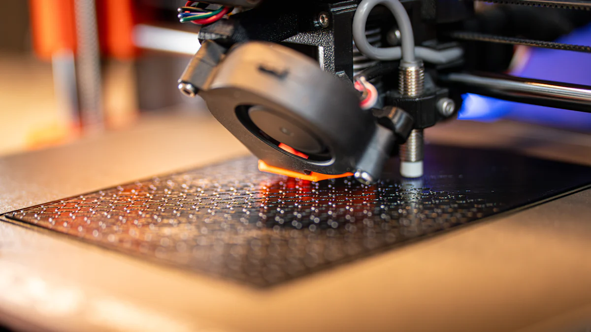
Practical Guide to Using Focused Electron Beam for 3D Nanoprinting
Focused electron beam technology plays a pivotal role in the realm of 3D nanoprinting. This guide provides a comprehensive overview of the practical steps and best practices for utilizing this advanced technology effectively.
Step-by-Step Process
Setting Up the Equipment
Setting up the equipment is the first crucial step in 3D nanoprinting. Operators must ensure that the electron beam system is calibrated correctly. This involves adjusting the electron gun to emit a focused beam with the desired intensity and precision. The vacuum chamber must be free of contaminants to prevent interference with the beam’s path. Regular maintenance checks are essential to keep the equipment in optimal condition, ensuring consistent performance during the deposition process.
Preparing the Material
Material preparation is vital for successful 3D nanoprinting. The choice of precursor materials significantly impacts the quality of the final structure. Operators should select materials compatible with focused electron beam induced deposition (FEBID) techniques. These materials must undergo thorough cleaning to remove impurities that could affect the deposition process. Proper preparation ensures that the material interacts effectively with the electron beam, allowing for precise manipulation at the nanoscale.
Tips and Best Practices
Ensuring Safety and Precision
Safety and precision are paramount in 3D nanoprinting. Operators must adhere to safety protocols to protect themselves from exposure to high-energy electron beams. Wearing appropriate protective gear and following established guidelines minimizes risks. Precision in beam control is equally important. Operators should regularly calibrate the equipment to maintain the desired resolution and accuracy. This attention to detail ensures that each layer of the 3D structure aligns perfectly, resulting in high-quality nanoprinting outcomes.
Troubleshooting Common Issues
Troubleshooting is an integral part of the 3D nanoprinting process. Operators may encounter issues such as beam misalignment or inconsistent deposition rates. Regular equipment checks can help identify and resolve these problems promptly. Adjusting the beam’s focus and intensity can correct alignment issues, while monitoring the deposition process ensures uniform material distribution. By addressing these challenges proactively, operators can maintain the integrity of the 3D structures and achieve the desired results.
“The development of electron beam technology has showcased unparalleled precision and control in manipulating matter at the atomic level.” — Scientists
Focused electron beam technology continues to revolutionize 3D nanoprinting. By following these practical guidelines, operators can harness the full potential of this technology, achieving remarkable precision and versatility in their nanoprinting endeavors.
Conclusion
Focused electron beam continues to redefine the landscape of 3D nanoprinting. Its transformative potential lies in its ability to create intricate 3D structures with remarkable precision. While the benefits are substantial, challenges such as equipment costs and material limitations persist. However, the balance between these factors drives innovation. Future prospects appear promising, with advancements like real-time visualization enhancing control over atomic-scale processes. The development of shape memory alloys and functionally graded materials further exemplifies the versatility of 3D-FEBID. As research progresses, focused electron beam technology will likely unlock new possibilities across various fields.