


Electron beam vapor deposition stands as a cornerstone in modern material science, enabling the creation of high-quality thin films with remarkable precision. This technique uses an electron beam to heat and evaporate materials, which then condense onto a substrate, forming dense and pure coatings. Industries rely on this method for its ability to handle high-melting-point materials and produce uniform layers. Recent advancements in electron beam evaporation have further enhanced its efficiency, allowing for faster deposition rates and broader material compatibility. These innovations are driving its adoption in sectors demanding high temperature thin film deposition, such as semiconductors and optics.
Key Takeaways
- Electron beam vapor deposition is a highly efficient method for creating high-quality thin films, crucial for industries like electronics and optics.
- The process operates in a vacuum, minimizing contamination and ensuring pure, dense coatings with superior adhesion.
- Recent advancements in equipment, such as multi-pocket crucibles and real-time monitoring, enhance deposition precision and productivity.
- The technique supports a wide range of materials, including high-melting-point metals and complex oxides, expanding its application potential.
- Emerging trends like plasma-activated systems and multi-material deposition techniques are set to revolutionize thin-film technology.
- Despite challenges like high initial costs, opportunities for innovation exist through simplified designs and automation, making the technology more accessible.
- Collaboration between researchers and industry can drive further advancements, unlocking new applications in fields such as renewable energy and nanotechnology.
Understanding Electron Beam Vapor Deposition
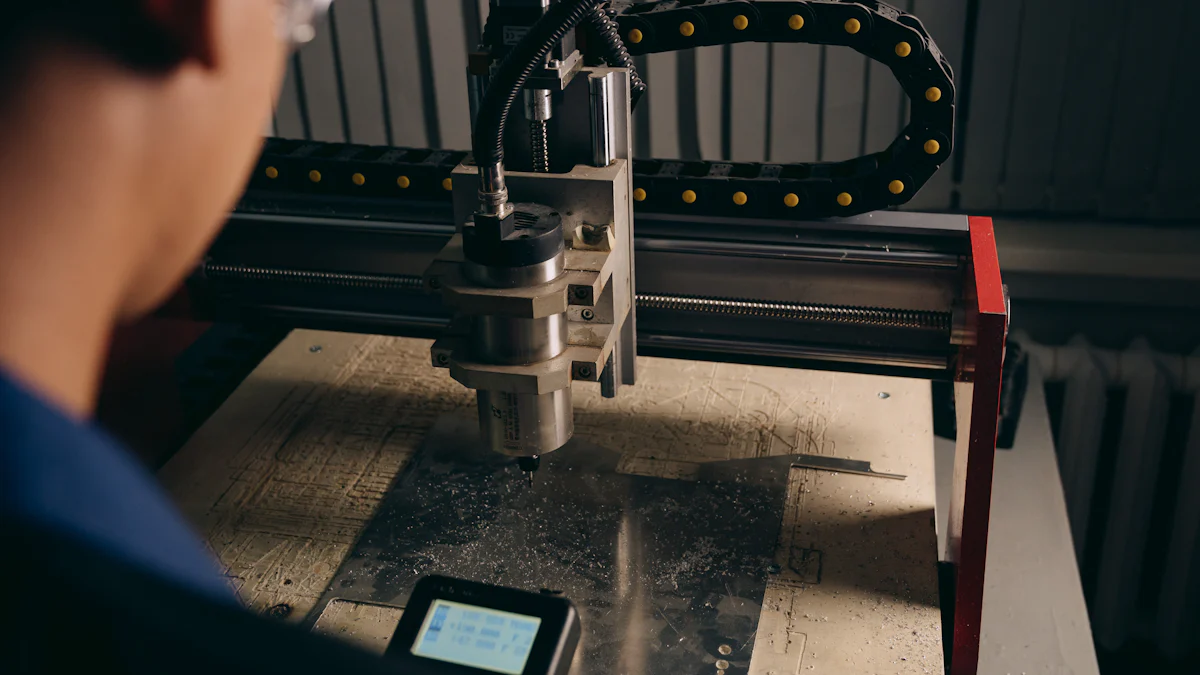
Electron beam vapor deposition represents a sophisticated method within the realm of physical vapour deposition. This process enables the creation of high-quality coatings by utilizing an electron beam to heat and evaporate materials. The vaporized material then condenses onto a substrate, forming a thin film. Industries value this technique for its ability to produce dense and uniform coatings, especially for materials with high melting points.
How Does Electron Beam Vapor Deposition Work?
The process begins with an electron beam directed at the target material inside a vacuum chamber. The beam transfers energy directly to the material, causing it to evaporate. The vacuum environment ensures that the vaporized material travels without interference, allowing it to deposit evenly on the substrate. This direct energy transfer makes the process highly efficient, particularly for metals and compounds with high melting points.
Unlike sputtering, which relies on ion collisions to eject material, electron beam evaporation achieves higher deposition rates. These rates can range from 0.1 nm per minute to 100 nm per minute, depending on the material and process parameters. This efficiency results in coatings with superior density and adhesion, making it ideal for applications requiring precision and durability.
Key Features of Electron Beam Vapor Deposition
Electron beam vapor deposition offers several distinct advantages:
- High Deposition Rates: The process achieves significantly faster rates compared to other physical vapour deposition methods. This efficiency reduces production time while maintaining quality.
- Material Versatility: It supports a wide range of materials, including metals, oxides, and semiconductors. This versatility expands its application across various industries.
- Precision and Uniformity: The process ensures even coating distribution on the substrate, resulting in thin films with consistent thickness and properties.
- Vacuum Environment: Operating in a vacuum minimizes contamination, enhancing the purity and performance of the deposited thin film.
- Energy Efficiency: Direct energy transfer from the electron beam to the material reduces energy waste, making the process more sustainable.
These features make electron beam vapor deposition a preferred choice for industries such as electronics, optics, and aerospace. Its ability to produce high-quality thin films with exceptional precision continues to drive innovation in material science.
Latest Advancements in Electron Beam Deposition Technology
Innovations in Equipment
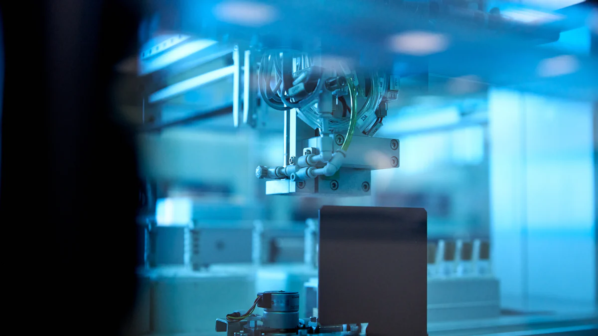
Recent innovations in equipment have significantly enhanced the efficiency and precision of electron beam evaporation. Modern electron beam evaporators now feature advanced control systems that allow operators to fine-tune parameters such as beam intensity, substrate rotation, and vacuum pressure. These improvements ensure better deposition uniformity and higher-quality coatings.
Manufacturers have also introduced multi-pocket crucibles in electron beam evaporators, enabling the use of multiple materials during a single deposition process. This advancement reduces downtime and increases productivity. Additionally, the integration of real-time monitoring systems provides immediate feedback on film thickness and deposition rates, ensuring consistent results across batches.
For instance, the development of plasma-activated electron beam deposition systems has further improved coating quality by enhancing the adhesion and density of thin films. These systems utilize plasma to activate the substrate surface, promoting better interaction between the vaporized material and the substrate.
These equipment advancements have made electron beam evaporation more reliable and versatile, meeting the growing demands of industries such as electronics, optics, and aerospace.
Advancements in Materials
The range of materials compatible with electron beam evaporation has expanded significantly. Researchers have developed techniques to deposit not only traditional metals but also complex oxides, semiconductors, and even nanostructured materials. This versatility has opened new possibilities for creating specialized thin-film coatings tailored to specific applications.
High-melting-point materials, such as tungsten and tantalum, are now easier to work with due to the precise energy control offered by modern electron beam evaporators. These materials are essential for applications requiring durability and resistance to extreme conditions. Furthermore, advancements in material science have enabled the deposition of multi-layered thin films, which combine different materials to achieve unique optical, electrical, or mechanical properties.
A notable breakthrough involves the use of electron beam chemical vapor deposition (CVD) for manufacturing nanomaterials. This technique allows for the creation of ultra-thin films with exceptional uniformity, making it ideal for next-generation electronic devices and sensors.
These material advancements have broadened the scope of electron-beam evaporation, making it a critical tool for industries seeking innovative solutions.
Cutting-Edge Techniques in Electron-Beam Evaporation
New techniques in electron-beam evaporation have revolutionized the thin-film deposition process. High deposition rates, achieved through optimized beam configurations, have reduced production times without compromising film quality. These rates, ranging from 0.1 μm/min to 100 μm/min, make the process highly efficient for large-scale manufacturing.
Advanced substrate manipulation techniques, such as dynamic rotation and tilting, have improved deposition uniformity. These methods ensure even coating distribution, especially on complex geometries. Additionally, innovations like reactive electron-beam evaporation allow for the in-situ formation of compounds during deposition. This technique is particularly useful for creating thin-film optical coatings with precise refractive indices.
The integration of ion-beam-assisted deposition systems has further enhanced the capabilities of electron-beam evaporation. By combining ion beams with electron beams, these systems improve film adhesion and reduce defects, resulting in superior coating performance.
These cutting-edge techniques continue to push the boundaries of what is possible with electron-beam evaporation, solidifying its role as a cornerstone of modern thin-film deposition technology.

Real-World Applications of Electron Beam Deposition
Electron beam deposition has become a vital technology across various industries. Its ability to create precise, high-quality thin films makes it indispensable for modern manufacturing and innovation. Below are some of the most prominent applications of this advanced deposition method.
Electronics and Semiconductor Applications
The electronics and semiconductor industries rely heavily on electron beam deposition for producing intricate and reliable components. This technology plays a crucial role in fabricating thin films used in microchips, transistors, and integrated circuits. The precision of deposition ensures uniform layers, which are essential for the performance and durability of these devices.
For example, the accuracy of lithography in semiconductor manufacturing directly impacts the efficiency of electronic devices. Better lithography leads to more powerful smartphones, dependable vehicles, and robust communication systems.
Electron beam evaporation applications in this sector also include the creation of nanostructured materials. These materials enhance the functionality of sensors and other electronic components, paving the way for advancements in consumer electronics and industrial equipment.
Optics and Photonics Applications
In optics and photonics, electron beam deposition enables the production of high-performance coatings for lenses, mirrors, and optical filters. These coatings improve light transmission, reduce reflection, and enhance durability, making them essential for applications in cameras, telescopes, and laser systems.
Physical Vapor Deposition (PVD), including electron beam methods, is widely used in this field to achieve superior surface properties. The precision of electron beam evaporation applications ensures that optical components meet stringent quality standards.
The technology also supports the development of advanced photonic devices, such as waveguides and modulators. These devices are critical for telecommunications, medical imaging, and other cutting-edge technologies.
Aerospace and Defense Applications
The aerospace and defense sectors benefit significantly from electron beam deposition. This method produces durable coatings that withstand extreme conditions, such as high temperatures and corrosive environments. These coatings are applied to turbine blades, engine components, and protective surfaces, ensuring reliability and longevity.
Additive manufacturing technologies, which have grown rapidly since the mid-1980s, often incorporate electron beam deposition for creating complex geometries. This capability is particularly valuable for aerospace applications, where lightweight and robust materials are essential.
In defense, electron beam evaporation applications extend to the production of thin films for sensors, radar systems, and stealth technologies. These innovations enhance the performance and effectiveness of military equipment, contributing to national security.
Future Potential of Electron Beam Deposition
Emerging Trends in Electron Beam Evaporation
Electron beam evaporation continues to evolve, driven by advancements in technology and material science. One significant trend is the increasing adoption of plasma-activated electron beam systems. These systems enhance the interaction between the substrate and vaporized material, resulting in coatings with improved adhesion and density. This innovation addresses the growing demand for high-performance thin films in industries like aerospace and electronics.
Another emerging trend involves the integration of real-time monitoring and control systems. These systems allow operators to adjust deposition parameters with precision, ensuring consistent results. For example, modern equipment now includes sensors that measure film thickness during the process. This capability reduces waste and enhances production efficiency.
The development of multi-material deposition techniques is also gaining traction. Multi-pocket crucibles enable the use of different materials in a single process, creating complex, multi-layered coatings. These coatings combine unique properties, such as enhanced optical performance or electrical conductivity, making them suitable for advanced applications in photonics and semiconductors.
A notable advancement is the use of reactive electron beam evaporation. This technique allows for the in-situ formation of compounds, such as oxides or nitrides, during the deposition process. It provides manufacturers with greater flexibility in tailoring thin films to specific requirements.
These trends highlight the potential of electron beam evaporation to meet the evolving needs of modern industries, ensuring its relevance in the future.
Challenges and Opportunities for Broader Applications
Despite its advantages, electron beam evaporation faces several challenges that could limit its broader adoption. The complexity of the equipment and the need for skilled operators increase operational costs. Small-scale manufacturers may find it difficult to invest in this technology due to its high initial setup expenses.
Material limitations also pose a challenge. While electron beam evaporation supports a wide range of materials, certain compounds may still require alternative methods. For instance, thermal evaporation remains more suitable for materials with low melting points, despite its drawbacks, such as higher contamination risks and less dense coatings.
However, these challenges present opportunities for innovation. Simplifying equipment design and automating processes could reduce costs and make the technology more accessible. Advances in material science may also expand the range of compatible materials, enabling the deposition of even more specialized thin films.
The versatility of electron beam evaporation offers a significant advantage over traditional methods like thermal evaporation. It allows for precise control over deposition rates and minimizes contamination, making it ideal for high-performance applications.
Collaboration between researchers and industry leaders could further drive innovation. By addressing existing limitations, electron beam evaporation can unlock new possibilities in fields such as renewable energy, medical devices, and nanotechnology. Its potential to revolutionize thin-film deposition remains vast, provided these challenges are met with creative solutions.
Conclusion
Electron beam vapor deposition has revolutionized thin-film technology with its precision, efficiency, and versatility. Its ability to achieve high deposition rates, ranging from 0.1 nm to 100 nm per minute, ensures superior coatings for diverse applications. Industries such as electronics, optics, and aerospace increasingly rely on this method for its unmatched material compatibility and energy efficiency.
As advancements continue, electron beam deposition holds immense potential to address emerging industrial challenges and drive innovation across sectors. Its future promises broader adoption and groundbreaking applications.