


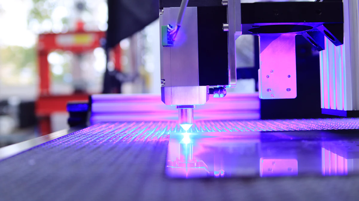
Electron beam lithography has revolutionized the field of microfabrication, playing a crucial role in the advancement of modern technology. The electron beam lithography history reveals how this technique allows for the precise manipulation and patterning of materials at the nanoscale, enabling the creation of intricate devices and structures with exceptional resolution. The demand for semiconductor devices with advanced functionality continues to drive the growth of electron beam technology. Its ability to produce nanoscale patterns is vital for fabricating integrated circuits, optoelectronics, and quantum technologies. As a cornerstone of nanotechnology, electron beam lithography remains indispensable in shaping the future of electronics.
Key Takeaways
- Electron beam lithography (e-beam lithography) is crucial for creating nanoscale patterns, enabling advancements in semiconductors, optoelectronics, and quantum technologies.
- The technique evolved from early experiments in the 1960s, showcasing the potential of electron beams to achieve high-resolution patterning beyond the capabilities of traditional optical methods.
- Significant advancements in the 1970s and 1980s, including high-speed and computer-controlled systems, enhanced the precision and efficiency of e-beam lithography, making it indispensable in modern manufacturing.
- The transition from research to commercial use has revolutionized semiconductor manufacturing, allowing for rapid prototyping and customization without the need for costly masks.
- Recent innovations, such as new resist materials and multiple-electron-beam systems, have increased the throughput and versatility of e-beam lithography, expanding its applications across various industries.
- Looking ahead, electron beam lithography is poised to play a vital role in emerging fields like quantum computing and advanced materials, driving future technological innovations.
- Addressing challenges such as operational costs and the need for specialized expertise will be essential for the continued growth and accessibility of electron beam lithography.
The Inception of Electron Beam Lithography
Early Concepts and Theoretical Foundations
The journey of electron beam lithography began with the exploration of electron beam technology in the late 1960s. Researchers sought to harness the precision of electron beams for patterning materials at a microscopic level. This period marked the adaptation of scanning electron microscopes into tools capable of performing lithography. The theoretical foundations laid during this time emphasized the potential of electron beams to achieve high-resolution patterning, which traditional optical lithography could not match.
The concept of using electrons for writing patterns emerged from the need to overcome the diffraction limits of light. Scientists realized that electrons, with their shorter wavelengths, could produce much finer details. This realization set the stage for the development of e-beam lithography, a technique that would revolutionize microfabrication. The early theoretical work focused on understanding how electron beams interact with materials, leading to the creation of models that predicted the behavior of electrons during the lithography process.
Initial Experiments and Prototypes
Initial experiments in electron beam lithography involved modifying existing electron microscopes to serve as lithography tools. These early systems demonstrated the feasibility of using electron beams for direct writing on substrates. Researchers conducted experiments to refine the control of electron beams, aiming to achieve precise patterning without the need for masks. This direct-write capability distinguished e-beam lithography from other lithography techniques, offering unparalleled flexibility and resolution.
Prototypes developed during this era showcased the potential of electron beam writing in creating intricate patterns. These prototypes paved the way for further advancements in electron beam technology, setting the foundation for modern e-beam lithography systems. The success of these initial experiments highlighted the advantages of electron beam lithography, such as its ability to produce nanoscale features essential for semiconductor manufacturing and other advanced applications.
Technological Advancements in the 1970s and 1980s
Development of High-Resolution Techniques
The 1970s and 1980s marked a period of significant progress in electron beam lithography. Researchers focused on enhancing high-resolution imaging capabilities, which became crucial for advancing microfabrication. During this era, scientists at institutions like MIT’s Research Laboratory of Electronics (RLE) achieved remarkable breakthroughs. They demonstrated advancements in high-speed e-beam lithography, achieving resolutions as fine as nine nanometers. This level of precision allowed for the creation of intricate patterns that were previously unattainable.
High-resolution imaging techniques evolved rapidly, enabling the fabrication of smaller and more complex structures. The ability to produce such detailed patterns revolutionized the semiconductor industry. It allowed for the development of integrated circuits with higher performance and efficiency. These advancements in high resolution also paved the way for innovations in optoelectronics and quantum technologies, where precise patterning is essential.
Introduction of Computer-Controlled Systems
The introduction of computer-controlled systems in electron beam technology during the 1980s further enhanced lithography processes. These systems provided unprecedented control over the electron beam, allowing for more accurate and efficient patterning. By integrating computers into the lithography process, researchers could automate complex tasks, reducing human error and increasing throughput.
Computer-controlled systems enabled the development of new techniques for creating patterns on uneven and nonplanar surfaces. This innovation surpassed the limitations of traditional e-beam lithography, which was primarily effective on flat surfaces. Researchers began exploring new alternatives for fabricating 3D nanostructures on rough surfaces, expanding the possibilities of electron beam technology.
The advancements in computer-controlled systems also contributed to the widespread adoption of electron beam lithography in various industries. As the technology became more accessible and reliable, it found applications in fields beyond semiconductors, including biotechnology and materials science. The ability to achieve high-resolution imaging with precision and efficiency made electron beam lithography an indispensable tool in modern technology.
Commercialization and Industry Adoption
Transition from Research to Commercial Use
Electron beam lithography transitioned from research laboratories to commercial applications, marking a significant milestone in its history. Initially, researchers focused on understanding the theoretical aspects and conducting experiments to refine the technology. As the demand for advanced semiconductor devices grew, the industry recognized the potential of electron beam lithography in commercial settings. This shift allowed for the development of microelectromechanical systems (MEMS) and nanoelectromechanical systems (NEMS), which benefited from the precision and flexibility of maskless lithography.
The collaboration between academia and industry played a crucial role in this transition. Academic institutions provided the foundational research and innovation, while industry partners contributed resources and expertise to scale up production. This partnership facilitated the commercialization of electron beam technology, enabling its widespread adoption across various sectors. The ability to produce intricate patterns without masks made maskless lithography an attractive option for manufacturers seeking to enhance their production capabilities.
Impact on Semiconductor Manufacturing
The impact of electron beam lithography on semiconductor manufacturing has been profound. As the technology moved into commercial use, it revolutionized the way semiconductors were produced. The precision of electron beam lithography allowed for the creation of smaller and more complex integrated circuits, which are essential for modern electronic devices. This advancement led to significant improvements in performance and efficiency, driving the growth of the semiconductor industry.
Maskless lithography offered several advantages over traditional methods. It eliminated the need for costly masks, reducing production costs and increasing flexibility. Manufacturers could quickly adapt to design changes, allowing for rapid prototyping and customization. This capability proved invaluable in an industry characterized by fast-paced innovation and evolving consumer demands.
The adoption of electron beam technology in semiconductor manufacturing also spurred further advancements in related fields. Researchers explored new materials and techniques, pushing the boundaries of what was possible with lithography. This ongoing innovation continues to shape the future of electronics, with electron beam lithography remaining a cornerstone of technological progress.

Breakthroughs in the 1990s and 2000s
Enhancements in Speed and Precision
The 1990s and 2000s witnessed remarkable advancements in electron beam lithography, particularly in terms of speed and precision. Researchers focused on overcoming the limitations of earlier systems, which often struggled with slow processing times. By enhancing the speed of electron beam technology, they significantly improved its efficiency, making it more viable for commercial applications.
Scientific Research Findings:
- Electron Beam Lithography Research Findings highlighted that electron beam lithography achieved lateral resolutions as fine as 10 nm. This level of precision marked a significant milestone in the field, allowing for the creation of intricate patterns with unprecedented detail.
- At MIT, researchers demonstrated advancements in high-speed e-beam lithography, achieving resolutions as fine as nine nanometers. These breakthroughs underscored the potential of electron beam technology to produce nanoscale patterns with exceptional accuracy.
The improvements in speed and precision enabled electron beam lithography to meet the growing demands of the semiconductor industry. As the need for smaller and more complex integrated circuits increased, electron beam technology provided a solution by delivering high-resolution patterns quickly and efficiently. This capability proved essential for the fabrication of advanced electronic devices, including microprocessors and memory chips.
Integration with Other Lithography Techniques
During this period, the integration of electron beam lithography with other lithography techniques emerged as a key trend. Researchers explored ways to combine the strengths of different methods to enhance overall performance and expand the range of applications.
One notable development involved the hybridization of electron beam lithography with optical lithography. By leveraging the high resolution of electron beams and the speed of optical systems, this approach offered a balanced solution for producing complex patterns. The integration allowed for the fabrication of features at the nanoscale while maintaining efficient throughput, addressing the limitations of each technique when used independently.
Additionally, the combination of electron beam lithography with nanoimprint lithography gained traction. This synergy enabled the replication of nanoscale patterns over large areas, making it suitable for mass production. The integration of these techniques facilitated the development of innovative applications in fields such as biotechnology and materials science, where precise patterning is crucial.
The breakthroughs in the 1990s and 2000s solidified electron beam lithography’s position as a cornerstone of modern lithography. By enhancing speed and precision and integrating with other techniques, electron beam technology continued to drive advancements in nanofabrication, paving the way for future innovations in electronics and beyond.

Recent Innovations and Current Trends
Advances in Nanotechnology Applications
Electron beam lithography has become a cornerstone in the field of nanotechnology. Researchers have harnessed its precision to create intricate nanostructures, which serve as the foundation for diverse applications. The ability to manipulate materials at the nanoscale has opened new avenues in fields such as medicine, electronics, and materials science.
- Medical Applications: Scientists use electron beam lithography to develop nanoscale devices for drug delivery and diagnostics. These devices can target specific cells or tissues, improving the efficacy of treatments and reducing side effects.
- Electronics: In the electronics industry, electron beam technology enables the fabrication of smaller and more efficient components. This advancement supports the development of faster and more powerful electronic devices, from smartphones to supercomputers.
- Materials Science: Researchers employ electron beam lithography to create novel materials with unique properties. These materials find applications in various industries, including aerospace and energy, where they contribute to the development of lighter and more durable products.
The fine control over nanostructure features provided by electron beam lithography continues to drive innovation. As scientists explore new possibilities, the impact of this technology on nanotechnology applications will likely expand further.
Emerging Materials and Techniques
The field of lithography has witnessed significant advancements in recent years, particularly with the introduction of new materials and techniques. These innovations have enhanced the capabilities of electron beam technology, allowing for more efficient and versatile patterning processes.
- New Resist Materials: Researchers have developed advanced resist materials that improve the resolution and sensitivity of electron beam lithography. These materials enable the creation of finer patterns, essential for the next generation of electronic devices.
- Multiple-Electron-Beam Systems: The introduction of multiple-electron-beam systems has increased the throughput of electron beam lithography. By using several beams simultaneously, these systems can pattern larger areas more quickly, making the technology more suitable for commercial applications.
- Hybrid Techniques: Scientists have explored hybrid techniques that combine electron beam lithography with other methods, such as nanoimprint lithography. This approach leverages the strengths of each technique, resulting in more efficient and cost-effective patterning solutions.
These emerging materials and techniques have positioned electron beam lithography as a vital tool in modern technology. As the demand for smaller and more complex devices grows, the continued evolution of lithography will play a crucial role in meeting these challenges.
The Future of Electron Beam Lithography
Potential Developments and Challenges
Electron beam lithography stands on the brink of transformative developments. Researchers anticipate advancements that will enhance its capabilities, making it even more integral to technological progress. Researchers at MIT’s Research Laboratory of Electronics (RLE) have already demonstrated significant improvements in high-speed e-beam lithography, achieving resolutions as fine as nine nanometers. This breakthrough underscores the potential for electron beam lithography to support mass production while maintaining the precision needed for prototyping.
- Increased Throughput: Future developments may focus on increasing the throughput of electron beam lithography. By enhancing the speed at which patterns are created, manufacturers can meet the growing demand for smaller and more complex devices.
- Improved Resolution: Achieving even finer resolutions remains a key goal. As technology advances, electron beam lithography could push the boundaries of what is possible, enabling the creation of features at the atomic scale.
- Cost Reduction: Reducing the cost of electron beam technology will be crucial for its widespread adoption. Innovations that lower production expenses without compromising quality will make this technology more accessible to various industries.
Despite these promising developments, challenges persist. The complexity of electron beam lithography systems can lead to high operational costs and maintenance requirements. Additionally, the need for specialized expertise in operating these systems may limit their use to certain sectors. Addressing these challenges will be essential for the continued growth and success of electron beam technology.
Role in Future Technological Innovations
Electron beam lithography will play a pivotal role in shaping future technological innovations. Its ability to create precise nanoscale patterns makes it indispensable for several emerging fields.
- Quantum Computing: As researchers explore the potential of quantum computing, electron beam lithography will be vital in fabricating the intricate components required for these advanced systems. The precision of electron beam technology ensures the accurate placement of quantum bits, or qubits, which are essential for the operation of quantum computers.
- Advanced Materials: The development of new materials with unique properties will benefit from electron beam lithography. By enabling the precise patterning of materials at the nanoscale, this technology supports the creation of materials with enhanced strength, flexibility, and conductivity.
- Biotechnology: In biotechnology, electron beam lithography facilitates the creation of nanoscale devices for medical applications. These devices can revolutionize drug delivery systems and diagnostic tools, improving patient outcomes and advancing healthcare.
The future of electron beam lithography promises exciting possibilities. As researchers continue to push the limits of this technology, its impact on various industries will only grow. By overcoming current challenges and embracing new opportunities, electron beam lithography will remain a cornerstone of innovation in the years to come.
Conclusion
The electron beam lithography history showcases a remarkable journey of technological evolution. From its inception, electron beam lithography has played a pivotal role in nanofabrication and nanotechnology. This technique enables the creation of advanced devices and structures with extraordinary precision and resolution. As electron beam technology continues to evolve, it remains essential for fabricating nano-scaled components crucial to tomorrow’s devices, especially in semiconductors, optoelectronics, and quantum technologies. The ongoing advancements in lithography promise to shape the future of technology, ensuring its relevance and impact for years to come.